▢ Co-Packaged Optics (CPO) for High-Speed AI Interconnects
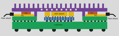
Co-packaged optics (CPO) combines advanced semiconductor packaging with optical interconnect technologies to enable high-bandwidth and energy-efficient communication for AI computing systems. Innovative packaging architectures, photonic integration, and optical I/O solutions are being developed to support next-generation AI data centers.
▢ Highly Reliable Solder Joint Interconnections
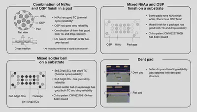
Solder joints are among the most widely used electrical interconnections in semiconductor packaging and heterogeneous integration. With increasing interconnect density and continuous scaling of solder joint dimensions in advanced packaging, achieving reliable and robust solder joint interconnections has become increasingly critical.
Relevant Publications and Patents
- Zhang, Jing, Hai Liu, and Jaisung Lee. “Board level cyclic bending test for MCP package.” In 2007 9th Electronics Packaging Technology Conference, pp. 459-462. IEEE, 2007.
- Liu, Hai, Jing Zhang, Song Chen, Maohua Du, Nufeng Feng, Qian Wang, and Taekoo Lee. “Board level thermal cycle reliability of BGA for a new type of pad structure with OSP surface finish.” In 2007 8th International Conference on Electronic Packaging Technology, pp. 1-3. IEEE, 2007.
- Liu, Hai. “Printed circuit board for semiconductor package.” U.S. Patent 9,504,152 B2, issued November 22, 2016.
- Liu, Hai. “Printed Circuit Board and Semiconductor Packaging Including It.” Chinese Patent 105307386 B, issued July 06, 2018.
- Liu, Hai. “A Mixed Surface Coating and Its Manufacturing Method.” Chinese Patent 103227160 B, issued March 16, 2016.
- Lu, Kai, and Hai Liu. “Mixed Solder Ball Arrangement and Its Formation Method.” Chinese Patent 103219310 B, issued July 13, 2016.
▢ Advanced Wire Bonding
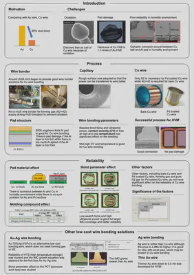
Cu wire bonding offers higher electrical and thermal conductivity at a lower cost compared to traditional Au wire bonding. However, it faces challenges such as bond pad damage during processing and reliability issues in humid environments. We addressed these issues through tailored material selection and process parameter optimization.
Relevant Publications
- Liu, Hai, Zhenqing Zhao, Qiang Chen, Jianwei Zhou, Maohua Du, Senyun Kim, Jonghyun Chae, and Myungkee Chung. “Reliability of copper wire bonding in humidity environment.” In 2011 IEEE 13th Electronics Packaging Technology Conference, pp. 53-58. IEEE, 2011.
- Chen, Qiang, Zhenqing Zhao, Hai Liu, Jonghyun Chae, Senyun Kim, and Myungkee Chung. “Investigation of various pad structure influence for copper wire bondability.” In 2011 12th International Conference on Electronic Packaging Technology and High Density Packaging, pp. 1-4. IEEE, 2011.
- Liu, Hai, Qi Chen, Zhenqing Zhao, Qian Wang, Jianfeng Zeng, and Jonghyun Chae. “Reliability of Au-Ag alloy wire bonding.” In 2010 Proceedings 60th Electronic Components and Technology Conference (ECTC), pp. 234-239. IEEE, 2010.
▢ Low Cost PCB and Substrate
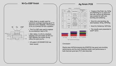
Development of innovative PCB and substrate surface finishes, including Ni-Cu-OSP and Ni-Pd-Ag, as cost-effective alternatives to conventional Ni/Au finishes while maintaining excellent solder joint reliability.
Relevant Publications and Patents
- Liu, Hai, Li Jin, Liqun Gu, Juanjuan Li, Ying Li, Qiang Chen, Maouha Du, Jianwei Zhou, and TaeSub Chang. “Solder joint reliability with various silver finish on PCB.” In 2014 15th International Conference on Electronic Packaging Technology, pp. 396-400. IEEE, 2014.
- Liu, Hai. “Methods of manufacturing printed circuit board and semiconductor package.” U.S. Patent 10,049,970 B2, issued August 14, 2018.
▢ Thin Stacked Die Packaging
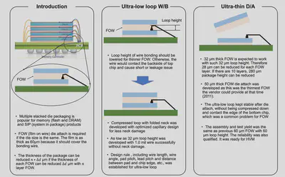
3D die stacking with wire bonding or TSV–solder interconnections enables high-density, high-speed memory for high-performance computing and data storage in desktop, mobile, automotive, and data center applications.
▢ Cavity Packaging for MEMS Ultrasonic Ranging Sensor
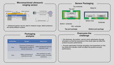
Packaging design, materials, and manufacturing processes play critical roles in determining acoustic performance.
▢ Wafer Level Chip Scale Packaging (WLCSP) for Wearable Fingerprint Sensor
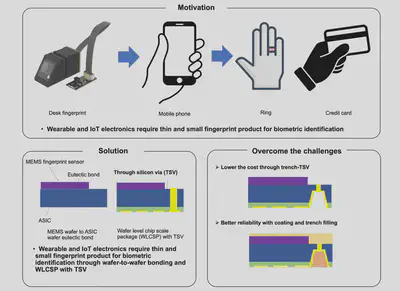
Development of ultra-thin MEMS ultrasonic fingerprint sensors for wearable electronics through wafer-level chip-scale packaging (WLCSP) with through-silicon vias (TSVs), enabling miniaturized, cost-effective, and highly reliable products.